Microchips
1 April 2023
There must still be some readers who remember their first electronic ignition. Come service time, you’d get out the timing light, loosen the distributor, twist it a bit this way and a bit that way and then tighten it up in exactly the same spot you started from. After one or two times, it became clear what a waste of time the procedure was. Such is the reliability of electronics. Since those days, more and more microchips have been incorporated in all vehicle systems.
Of course, automotive chips have been a bit thin on the ground over the last couple of years. Some figures show new car production was down by about 10 million units in 2021, four million in 2022 and, this year, the industry will still turn out three million fewer cars because of the chip shortage. Microchips themselves are obviously complex, so is their manufacture, so are the economics surrounding them and so is the geopolitical environment in which all this occurs.
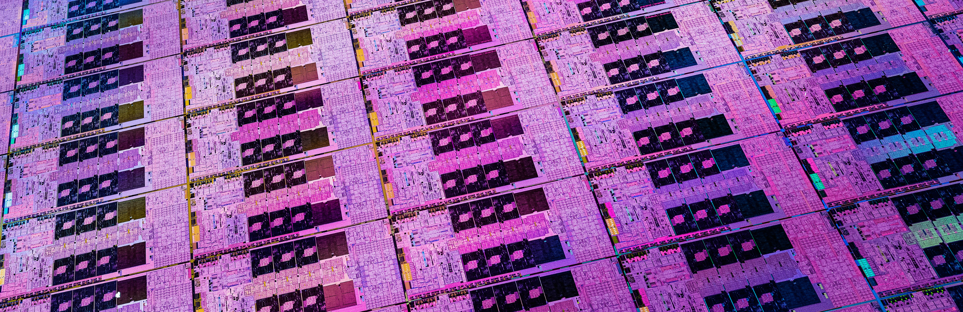
Chips are manufactured in hyper-clean factories known as fabs (fabrication facilities or foundries), in industry jargon. Taiwan has most of the high-end foundries but the industry is much more complex than that. Even though Taiwan makes most of the world’s most advanced chips, it’s US companies that design the circuitry on the chips and create the software used to do so. Japanese companies are the main source of the silicon wafers used, while a company called ASML in the Netherlands makes the laser etching machines used by fabs around the world. ASML is the only company in the world that makes machines capable of creating the most advanced chips.
What does advanced mean?
Microchips are broadly defined by what’s known as their minimum feature size, expressed in nanometres (nm). Feature size can refer to a number of things, but often it’s transistor gate size, or at least it was. Exactly what it means these days doesn’t really matter. Just know that smaller is better.
How small is small?
A nanometre is a billionth of a metre or one millionth of a millimetre. The most common sizes in use today for advanced chips is either 10nm or 7nm but some manufacturers produce 5nm or even 3nm units. Back in 2021, IBM created a 2nm chip, which is still in development. There’s even a 1nm chip, but it’s still in the research phase.
For some perspective on all these nanometres, consider that the average human hair is about 90,000nm thick. The diameter of the smallest virus is about 14nm (depending on who you ask), while DNA is about 2nm. So a 1nm or 2nm chip is vanishingly small. For that matter, so is a 10nm or 20nm chip. These sizes and the technologies that create them are collectively referred to as nodes. To maintain some perspective, though, it’s important to note a 5nm microchip doesn’t have twice as many transistors as a 10nm node.
Where do automotive chips sit in all of this? Automotive chips range from 90nm down to 40nm in size. Why are they so large compared with the latest advanced chips? Well, automotive chips don’t have the same need for miniaturisation as phones or other compact devices. The industry settled on this size range decades ago and there’s been no need to change it. Doing so wouldn’t have much practical benefit in a car and would cost much more. The sunk costs for fabs and associated technologies that create automotive microchips were amortised decades ago and, of course, one of the main pressures in automotive manufacturing is cost reduction. Given the number of chips consumed by the automotive sector, a saving of just one cent on each of them could result in the saving of many millions of dollars. But there’s more to it than that.
A vehicle is a challenging environment for a microchip. Temperature and vibration are two of the most difficult problems. An automotive chip might have to operate in conditions from well below zero to considerably more than 100 degrees Celsius. And dealing with vibration calls for more robust interconnects, both within a chip and peripheral to it. That means a bigger chip.
Because automotive microchips are often used in safety critical applications, they must be extremely reliable. Such chips are arduously tested under extreme conditions. Also, the fabs and processes used to produce them are certified to do so. This certification process can take months. Overall, a new automotive chip can take years to design, develop and certify before being used in a vehicle. The automotive microchip industry simply can’t respond or scale up production quickly.
This is essentially why auto manufacturers are experiencing a chip shortage. When they suspended orders as a consequence of COVID-19, fabs took orders from elsewhere, which tied up production capacity. Returning to the pre-pandemic status quo has been difficult. The shortage is easing, but production capacity, technical complexity and market forces have made the process slow. Still, most of that is probably pretty common knowledge by now.
Aside from feature size, microchips are defined by the size of the silicon wafers upon which they’re built. Technical progress in wafers is defined by increasing size rather than size reductions, as with individual chips, or dies as they’re called when they’re cut from wafers. Automotive chips are made on 200mm wafers. Again, this is old, established, fully depreciated technology. The most modern chips are made on 300mm wafers and 450mm wafers are in development.
Larger wafers are more economical but more technically difficult to use. This is easier to understand when you consider each wafer can undergo more than a thousand steps to build up the many layers modern chips have. Each wafer remains in the production stream for an average of 12 weeks from start to finish.
Casual consideration of wafer size belies the complexity of changing from one size to another in production. The equipment needed to manufacture microchips is tailored to a particular wafer size. Moving from 200mm to 300mm wafers cost the industry billions of dollars. While lower tech microchips are inexpensive, creating new manufacturing plants to make them is still very expensive. Also, they have the lowest profit margins. Fabs, in general, are expensive and those equipped to manufacture the most advanced chips cost multiple billions of dollars.
So, if microchips are square, why are wafers round? Doesn’t that waste a lot of space at the edges? There are two main reasons. First, silicon ingots (known in the industry as boules) are grown by slowly drawing them out of a crucible of molten silicon. This is done so each ingot is comprised of just one single silicon crystal with virtually no defects or inclusions. Silicon grown this way naturally takes a cylindrical form. Second, the coatings applied to silicon wafers are spin deposited, so a round wafer helps achieve an even coating, which is essential. A square wafer would definitely result in an uneven coating. In turn, this would result in a high reject rate for the chips, or dies, cut from the wafer.
The fact hundreds of dies are formed all over a wafer begs the question, can a wafer be processed to make a single gigantic chip? Such chips can, and are, made but they mitigate one of the main purposes of microelectronics – miniaturisation. Although such a chip won’t fit into a phone, there are applications in which these chips have a useful function. The technology is called WSI (Wafer Scale Integration) and a US company called Cerebras manufactures a wafer sized chip called WSE-2 (Wafer Scale Engine). It’s built for AI processing and Cerebras says it’s the fastest AI processor in existence.
Despite the purity of materials used in chip manufacturing and the ultra-cleanliness of the fabs, defects do occur on dies, always. Optical inspection can find defects at wafer level but, for minimum feature level inspection, other techniques are used. For conventional multi-die wafers the reject rate might be five per cent, however some sources say defect rates are often much higher. A Cerebras employee stated the WSE product mentioned earlier also has defects but that the chip was designed from the outset to have alternate paths around defect sites. This is a strategy used with individual dies, too.
The US invented microchips and originally dominated manufacturing. However, free markets generally move towards greater production efficiency. What’s more, free markets don’t care about political concerns.
As we said, microchip manufacturing is a globally dispersed industry in which companies in various countries have settled into specialised tasks. Back in the late 1980s the government-subsidised Japanese chip industry started growing and competing with the American industry, so the Americans effectively banned Japanese chips. The Japanese moved to specialising in the production of wafers.
The Taiwanese, on the other hand, decided to simply build fabs and make chips, and only chips. Again, this was government-subsidised, but it didn’t bother the Americans too much because it freed them from the expense of building very expensive fabs. The US still controlled the software and design without which Taiwan couldn’t make chips: a symbiotic rather than competitive relationship. The largest Taiwanese chip manufacturer is TSMC (Taiwanese Semiconductor Manufacturing Company), but it can’t make the machines that it uses to make the chips. It has to purchase them from the Netherlands.
Dutch company ASML is the only company in the world that builds machines to make the most advanced chips. This is because ASML developed them first and has been developing new processes and making iterative improvements to them for nearly four decades. Currently, the most advanced technology for making cutting edge chips is EUV lithography. The machines that do this are worth a couple of hundred million dollars each and ASML is selling them as fast as they can make them.
If manufacturing something as small is 2nm is impressive, the fact many billions of such elements all work together on a microchip is truly staggering. The human mind cannot design or even understand such a thing. That’s why the design software is so important. Fitting ever more transistors on smaller and smaller microchips is the name of the game, and it’s a game in which the US intends to rebuild its domination and maintain it, at China’s expense.
China is obsessed with Taiwan for a number of reasons. The One China policy is the best known, but another extremely important factor is microchip manufacturing. China manufactures lots of chips but they’re lower order types used in comparatively simple devices like microwave ovens, refrigerators, alarm clocks, etc. This is known as trailing edge technology as opposed to leading, or cutting edge technology.
China doesn’t yet have the expertise, equipment or software to manufacture higher level, leading edge chips used in things like the latest high-end phones, AI applications and, most importantly, advanced weapons. Both Taiwan and South Korea can, but it’s Taiwan that makes more than 90 per cent of the world’s most advanced microchips. It’s able to do so because of its symbiotic relationship with the US in the field of chip manufacturing.
China wants to get hold of the technology bound up in those fabs while the US is adamant they must not. In fact, limiting Chinese microchip technology was a large part of what the whole Huawei kerfuffle was all about some years ago. Taiwan manufactured the advanced chips for Huawei equipment, but the US didn’t like that and put a stop to it.
The US is currently using its strong influence to block companies around the world from supplying China with the technology it needs to make its own advanced chips, including ASML lithography machines from the Netherlands. It has also banned the sale of complete leading edge chips to China.
At the same time, the US Federal Chip and Science Act of 2022 allocates $280 billion dollars to technological development of which about $70 billion is designed to help US tech companies rebuild complete cutting edge microchip development and manufacturing on American shores. TSMC intends to be part of this and has started work on a new cutting-edge fab in Arizona, which is where IBM also has one. It must be said, though, the company is also building other fabs around the world.
By the end of the decade, the microchip industry is predicted to be worth $1 trillion. While the US sees complete self-sufficiency in semiconductor technology as a commercial imperative, strategic defence concerns are at least as important. It also wants to insulate itself from supply chain disruptions like those of the last couple of years.
As featured in Australasian Automotive April 2023.
912